Cdscdk2003 cd cadence. Jitter Due to variation in control voltage Due to uncertainty involved in.
Cadence Ic615 Virtuoso Tutorial 9 Noise Analysis In Cadence Adel Youtube
Jitter is usually a time domain term while phase noise is a frequency domain term.
. Phase noise and jitter in digital electronics are unavoidable but you can design to minimize things like power dropout crosstalk reflections and EMI susceptibility with a complete set of system analysis tools from Cadence. Your paths may be different depending on the class or project you are working on. Simply run a transient analysis and after the PLL is locked apply the eye diagram function form the calculator in cadence.
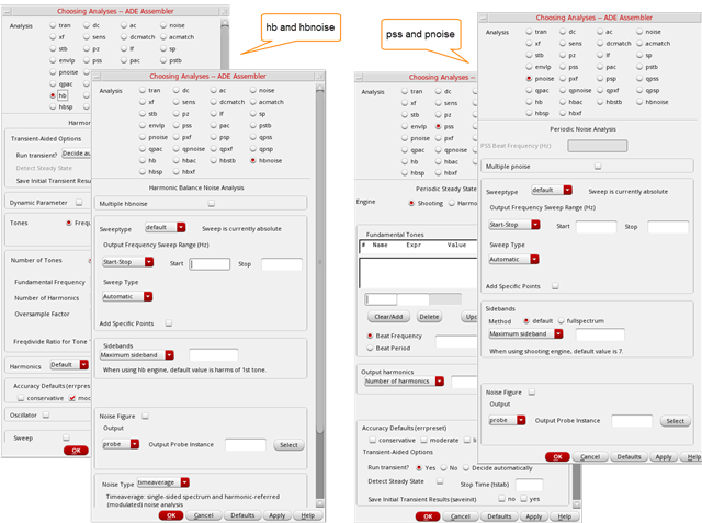
If you didnt save the previous dc simulation then follow the instructions in the previous tutorial to setup the dc simulation. Demystifying Noise Simulation in RF Circuits Spectre APS and RF Option. Improvements to PnoiseHbnoise Analysis in MMSIM151 and IC617ICADV122.
Start ADE by Tools-Analog Environment. Subscribe to our newsletter for the latest updates. 2 Table of Contents Types of Jitter Random Jitter Deterministic Jitter Correlated and Uncorrelated Jitter.
Timing Jitter Tutorial Measurement Guide Silicon Labs Timing. This tutorial provides a detailed guide to analysis and simulation of mixed-signal circuits like voltage-controlled oscillators VCOs used in clocking circuits for high-speed link applications. Start System requirement Statistical analysis include process mismatch effects.
This tutorial explains the procedure for plotting an eye diagram in Cadence. Also note that you can find additional tutorials and notes on the web from courses at other universities. Compared to that the difference of certain jitter types is almost negligible.
31 PM Jitter PM jitter is a non-accumulating jitter exhibited by driven systems. For more information on Cadence products and services. Environment ADE analog simulation tool.
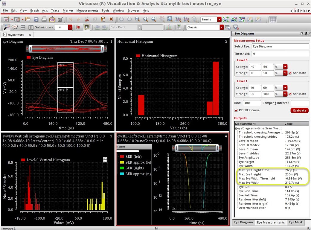
Cadence Tutorial 2 The following Cadence CAD tools will be used in this lab. Here you can select the Eye Diagram and define the Threshold. All parameter sets to their.
Please revisit Tutorial 1 before doing this new tutorial. This tutorial demonstrates the procedure for Post-layout simulations in Cadence and finding the number of parasitics in our layout. Analog Artist Spectre for simulation.
Another way to get jitter is by the eye diagram. Virtuoso Schematic for schematic capture. Simple test benches to perform analysis covered in this tutorial are discussed here.
For a single ended circuit say operational ampli ers a sample test circuit is shown in Fig. Id like to match simulation and measurement results. Yes Im interested in period jitter because we measured this type of jitter with a scope in the transient domain.
To do this we will load the previous dc simulation that we ran and add a transient simulation to it. Running the Cadence tools Please setup your environment then go to your cadence directory and start icfb. My problem is that the simulated amount of jitter largely depends on the simulation setup.
Oscillator Simulation on Cadence 6. Plot an eye diagram and choose the Eye Measurements tab. The threshold is the Y-axis voltage level and is generally half of the signal range.
Do tran analysis first to estimate the VCO frequency at the fixed Vctrl as the Beat frequency. If you tick the Plot BER Curve option you will get a Bit. Cadence simulation setup Monte Carlo Typical Model File Process Section 1.
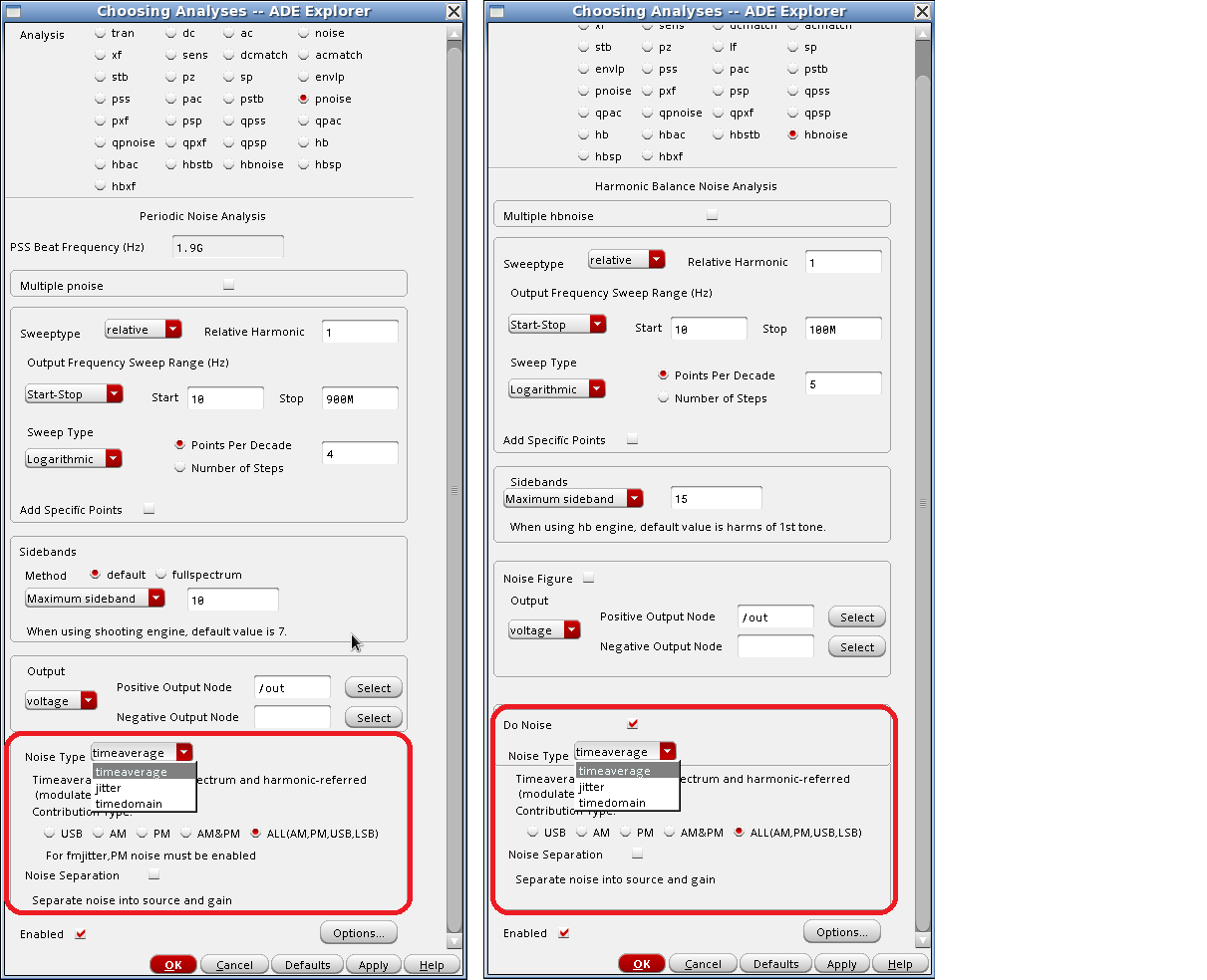
PM jitter is a random fluc-tuation in the delay between the input an d the output events. The Level 0 and Level 1 areas can be annotated by checking the Annotate check box. KVCO simulation PSS Periodic Steady State Analysis Any Verilog-A models are not allowed in the simulation bench PSS does not support Verilog-A.
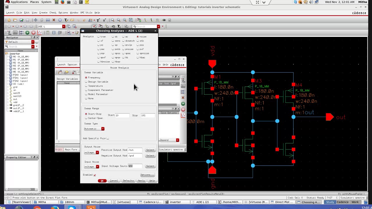
Tutorial B and C cover other Cadence tools important for custom IC design. In the PLL the PFD CP and FDs all exhibit PM jitter. In this tutorial the procedure for doing noise analysis in ADEL is explained.
In these components an output event occurs as a direct result of and some time after an input event. Moreover a brief overview of the eye diagram is given. The wide area in the eye diagram is the peak to peak jitter.
Load your final state from the first tutorial with Session -Load State. Comparing PnoiseHBnoise simulation results in the new MMSIM151IC617ICADV122 GUI to previous versions. A VCO model in Verilog-A is presented and a step-by-step guide to transient reponse and jitter calculation using Cadence Virtuoso IC616 is provided.
Virtuosity New Eye Diagram Measurements Custom Ic Design Cadence Blogs Cadence Community
2

Cadence 6 Tutorial 3 Youtube

Cadence Ic615 Virtuoso Tutorial 18 Eye Diagram In Cadence Ic615 Youtube
Measurement Of Phase Noise In Oscillators Rf Design Cadence Blogs Cadence Community
Noise Simulation In Spectre Rf Using Improved Pnoise Hbnoise And Direct Plot Form Options Rf Design Cadence Blogs Cadence Community

Cse 493 593 Cadence Tutorial
2
0 comments
Post a Comment